
Detectors of Light
- Page ID
- 338
The human eye is a low resolution detector of white visible light. Most well-resolved light detectors are essentially photon transducers, or instruments that detect electromagnetic radiation, and convert it into an electrical signal which can be amplified and transformed into an interpretable spectrum. An array of detectors exist, covering the various regions of the electromagnetic (EM) spectrum, but this module only discusses photon detectors for ultraviolet, visible, and near infrared radiation.
Introduction
Light has a dual nature, exhibiting both wave and particle like behavior. Here, light will be treated quantum mechanically, and represented as a particle phenomenon where it exists in packets of energy called photons. A photon has a discrete energy of
E = hc/\(\lambda\)
where h is Planck's constant (= 6.626 x 10⁻³⁴ J s), c is the speed of light (= 2.998 x 10⁸ m s-1), and \(\lambda\) is the wavelength of the EM wave. Photoelectric detectors are the main detectors used in the visible and ultraviolet regions of the EM spectrum. Phototubes and photodiodes make up one main class of photodetector types, and they are based on the photoelectric effect, which states that an electron will be liberated from a metal surface if the energy of the photon striking the surface is greater than the the work function of the surface. A liberated electron's maximum kinetic energy is given by
KEelectron = hv - \(\phi\)
where v is the frequency of the EM wave, and \(\phi\) is the work function of the metal surface. The lower the work function is, the easier it is to eject an electron. Therefore, materials with low work functions are employed in photodetectors.
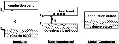
Another principle photodetector type is semiconductor based. When the energy of a photon is greater than that of the bandgap energy of a semiconductor material, then the photon energy is sufficient to break a bond and lift an electron into the conduction band. This creates an electron-hole pair that will allow current to flow (see Figure 2, middle), and detection occurs by measuring the current intensity.
Parameters that Characterize Good Detectors
Spectral Bandwidth
Spectral bandwidth refers to the wavelength range over which photons can be detected. Before light reaches the detector, it passes through a monochromator. It may be helpful here to briefly review the details of spectrophotometry. When a monochromator is set to a particular wavelength, light will come out at the exit slit with a Gaussian profile. Figure 1 shows a distribution of the light intensities that reach the sample, and on the figure \(\lambda\)* is the set wavelength. The spectral bandwidth is defined as the width of the band of light at the full width at half maximum (FWHM).
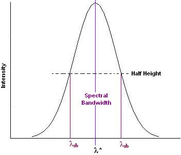
The spectral bandwidth of a spectrophotometer is related to the physical slit-width of the monochromator, and thus, to the instruments resolution capabilities. By optimizing the spectral bandwidth, one can optimize the resolution. Resolution here refers to how well the spectrophotometer can separate light into distinct wavelength regions that vary from one another.
Quantum Efficiency
The quantum efficiency, \(\eta\), for a photodiode is generally a function of wavelength, and is defined as
\(\eta\) = Number of photoelectrons liberated/Number of incident photons
The value of \(\eta\) for a detector is determined by the conduction and light absorption properties of the material is made of. The solid state properties will be discussed. Good photodetectors are those that have large values for \(\eta\). If \(\eta\) is low, it means that the incident photons are not being absorbed. Due to the non-directional nature of photoexcitation, an excited electron can move in any possible direction, and will not necessarily move towards the material that can liberate electrons if provided with enough energy. Instead, a significant number of excited electrons will lose their energy through premature scattering. Therefore, the quantum efficiency is limited by the non-directional nature of the excitation light.
Spectral Response
The wavelength of incident light affects the amount of current generated by the photodiode. For example, silicon photodiodes see a response from the UV/Visible regions, and even into the near infrared. Spectral response can be characterized by the short-circuit photocurrent generated by the photodiode divided by the energy, or power, of the incident light. The value obtained is called the radiometric sensitivity, and is mathematically given by
SR = ISC / \(\phi\)
where SR is the radiometric sensitivity in Amps/Watts, ISC is the short-circuit photocurrent in Amps, and \(\phi\) is the radiant flux in Watts.
Noise and Signal-to-Noise Ratios
A good detector detector exhibits high signal to noise ratios. The various types of noise present in photodetectors are discussed below.
Photon Shot Noise
Since current is carried by discrete charges, namely electrons, the current flowing through electrical conductors will undergo random fluctuations, and give rise to a type of background called shot noise. This is especially predominant in semiconductor diodes that rely on p-n junctions. Shot noise is given by
<I2noise> = 2q2 \(\phi\) \(\eta\) df
where q is the charge of an electron. From the formula, shot noise is proportional to the square root of the signal.
Dark Current Noise
So far, light energy has been introduced as a way to liberate electrons from a metal. Electrons can also be liberated by thermal energy, and since all molecules have a blackbody curve, they possess thermal energy even at room temperature. If that energy happens to be enough to excite electrons within the molecule into excited states, they may fluoresce if they are not non-radiatively deactivated as they relax back down to the ground state. This will lead to a background noise present in the absence of an excitation light source. Dark current noise can be greatly reduced by decreasing the temperature to help eliminate as much thermal motion as possible.
Read-Out Noise
Read-out noise is caused by the electronics in the CCD (charge-coupled device) output transistor and in the external circuitry. The CCD electronics do not measure the amount of charge in each packet of electrons perfectly. A small, but measurable amount of noise is added during the measurement process. This noise is termed read-out noise, and is expressed in units of electrons. Typically, the read-out noise for a CCD is around two to three electrons.
Thermal Noise
In a conductor, charge is completely free to move. Again, everything has a blackbody curve, and thus possess thermal energy at room temperature, and below. Thermal noise, also known as Johnson-Nyquist noise, is caused by the thermal (random) movement of the charge carriers inside the conductor. This electrical noise is inherent, and is present in all conductors (i.e. totally independent of the resistance). The formula for noise power is given by
P = kBTb
where P is the total noise power, k is the Boltzmann constant (= 1.38065 x 10⁻²³ J/K), T is the temperature, and b is the bandwidth.
General Recombination Noise
General recombination noise arrises from fluctuations in the number of conduction band electron holes and valence band holes available to conduct flow of electric charge. The photocurrent passing through the conductor material will have pulses that fluctuate randomly to cause general recombination noise.
Response Time
Response time essentially refers to time resolution, and refers to the minimum time interval over which changes in photon rates are detectable. Three main factors controlling the response time of a photodetector include the amount of time photocarriers spend in the depletion region, the diffusion time of photocarriers outside the depletion region, and the RC time constant of the circuit. The time spent in the depletion region depends on the carrier drift velocity, vd, and the width of the depletion layer, w, and is given by
td = w/vd
There is a trade-off between quantum efficiency and response time.
Linearity
It is desirable for the response to be linearly proportional to the incident photons. In a detector with linear response, the sensitivity remains constant at all sample concentrations. Examples of linear detectors are the photomultiplier tube and the CCD.
Dynamic Range
Dynamic range refers to the maximum variation in signal over which the detector output can represent photons without loss of signal. It is optimal to maximize the ratio of the largest measurable value to the smallest value.
Solid-State Properties
Semiconductors play an important role in detecting light. Figure 2 shows band diagrams of an insulator, semiconductor, and a conducting metal. The valence states and conduction states can be seen as ground and excited states of an atom. In order for charge to flow, there must be available states in the conduction band. Since the band gap is very large for the insulator, no charge will flow because there is not enough energy. The states overlap in the conductor, so charge flows very easily. However, in the semiconductor, which is more like an insulator, the band gap is relatively small. Therefore, electrons can be elevated into the conduction band much more easily than in the case of the insulator. This will leave holes in the valence band, which are effectively positive charge. When these holes are present in the material, charge can flow, and a current can be detected.
Photon Detectors
Vacuum Phototubes
The vacuum phototube is a very basic photon-detecting deviece that consists of two metal electrodes with a high voltage in between them, and it operates based on the photoelectric effect. Briefly, incident photons strike a photocatchode, and generate electrons that are attracted to an anode. Although phototubes do not have the dynodes, as shown in Figure 3, the operating principles are essentially the same, aside from the amplification factor.
Photomultiplier Tubes
Photomultiplier tubes (PMT's) utilize the photoelectric effect and the secondary emission of electrons to provide high current gains upon initial detection of a photon. Briefly, incident photons are directed towards a photocathode made up of a low work-function metal or semiconductor material. If the photon energy is greater than the work function of the cathode material, an electron has a high probability of being liberated from the material's surface. Once the electron is ejected from the cathode, it is accelerated by an applied electric field towards a series of dynodes, or electrodes. The dynodes are coated with a material that is likely to generate secondary emission of electrons and they are connected in series between resistors, causing a negative bias to form along the dynodes. The number of electrons quickly multiply through secondary emission, and this leads to an electrical current, which can be further amplified using an operational amplifier.
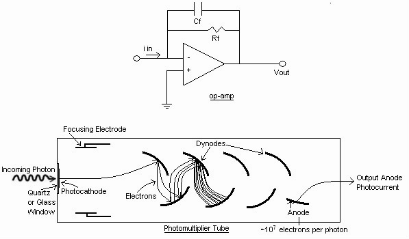
The PMT is extremely sensitive, and thus useful when a very low flux of photons is being measured. Even single photons yield measurable pulses with relatively high quantum efficiency. A disadvantage to this is that exposure to even low levels of light can destroy an operating PMT.
Photodiodes
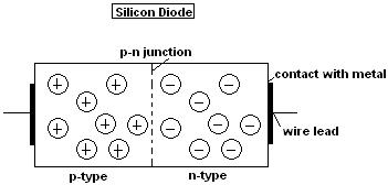
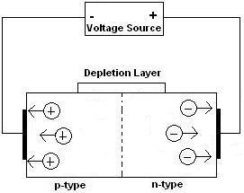
Photodiodes involve a p-n junction, which consists of two semiconductor materials that are oppositely doped. P-type refers to a positively doped semiconductor, while n-type refers to a negatively doped material. When the oppositely doped regions are place next to each other to create the junction, holes near the junction will tend to move across to the N-type space, while electrons in the N-type space will move towards the p-type space to occupy some of the holes. Thus, charge flow in a diode not connected to a battery will quickly come to a stop because the potential barrier builds up due to the charges that already migrated to opposite regions. No current will flow without placing a bias on the system. Now if a potential is placed across the material, then you will either have forward or reverse bias. If the positive side of the battery is connected to the p-type and the negative end to the n-type, then the electric field from the external potential difference can easily overcome the small internal field in the depletion zone that was caused by the initial drifting of charges. An applied field then attracts electrons to flow from the n to the p-type space and more holes from the p to the n-type space. This forward biased situation is a working diode. A second situation can arrise if the batter were to be switched so that the positive end was connected to the n-type rather than the p-type. Here, an external field will push electrons back into the n-type space while more holes move to the p-type space. This results in not net current flow, unless the reverse bias becomes so large that avalanche break down occurs to give current flow in the opposite direction. Depending on the wavelengths of interest, different semiconductor materials are used in constructing photodiodes. To observe photocurrent, the light energy provided must be sufficient to excite electrons across a material's bandgap. Silicon and Germanium are two materials that are used often, and they cover wavelength ranges of 190-1100nm and 400-1700nm respectively. Silicon is use most commonly because it has a greater bandgap, and therefore produces less dark current noise.

Charge-coupled Device (CCD)
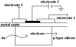
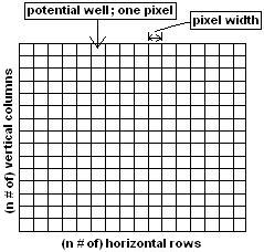
A CCD essentially operates in the same manner as a silicon photodiode, except that an array of potential wells with n number of rows and columns are involved. When photons hit the surface in a CCD, they are converted into an electric charge pattern. Figure 7 gives an illustration of the CCD cross section. Three electrodes are involved, two of which assist only with transferring charge. When a positive voltage is applied to the third electrode, the negatively charged electrons are attracted by the positively charged potential towards the electrode. Positively charged "holes" as seen in Figure 2 of the solid state properties section are repelled from the negatively charged area, thus creating a potential well where electrons are stored. The potential wells are grouped in a fixed pixel array, and so each pixel represents a set of charge that will come out together to be converted into a voltage. The pixels, or potential wells, are shown in Figure 8. As an increasing number of photons hit the CCD, the potential well surrounding the electrode attracts more electrons, up until the point where the well is completely saturated (filled) with charge. The charge pattern is slowly moved towards the output by changing the potentials of the wells. The coupled charge patterns are read out, set by set, or column by column, until the last column is read. The resolution of a CCD depends on the pixel width as well as the pixel separation, which is defined as the distance from the center of one well to the the center of an adjacent well.
References
- R. George, Detection of Light From the Ultraviolet to the Submillimeter, 2nd Edition (2003)
- D. Skoog, F. Holler, S. Crouch, Principles of Instrumental Analysis (2007)
Outside Links
- http://hyperphysics.phy-astr.gsu.edu...c/photdet.html
- en.Wikipedia.org/wiki/Photodiode
- en.Wikipedia.org/wiki/Photomultiplier
- en.Wikipedia.org/wiki/Charge-coupled_device
- en.Wikipedia.org/wiki/Pn_junction
Problems
- How would you construct a diode? Is a potential needed to make charge flow? What direction does the potential need to be for current to flow?
A semiconductor material such as silicon must be doped with a material of one charge less and one charge more to create p and n type materials. When placed adjacent to each other, they form a p-n junction, which when connected to a battery with the positive side connected to the p-type material, will give forward bias. - Why can't a conductor be used in constructing a diode?
Conductors reflect better than they absorb. - Define dark current, and how you would reduce it.
Dark current arises from the fact that everything has thermal energy, and this thermal energy is sometimes enough to promote electrons to higher energy states from which they must return to the ground state. If they do so by way of a radiative process like fluorescence, then a background noise signal will be detected. This can be reduced quite a bit by cooling the detector. - What are some disadvantages of the vacuum phototube and the photomultiplier tube?
Both devices are sensitive to low intensities, and have a fast response. However, they both cause a lot of light damage to the sample. Another disadvantage is that the semiconductor material only conducts under certain conditions. In the case of reverse-bias set up, no current will flow. - How is quantum efficiency related to spectral response?
The quantum efficiency is the number of liberated electrons compared to the number of incident photons, while the spectral response is the ratio of the generated current to the incident power.
Contributors and Attributions
- Jennifer Lien